Introduction to 128, 128L, 128LC2C Product Line for Film Stress Measurement
128 128L 128LC2C薄膜应力测试产品简介
128, 128L, 128C2C Product Line Introductions介绍
• Product Pictures产品图片
• Basic principles of 128 Line 128产品系列基本原理
• Film Stress薄膜应力
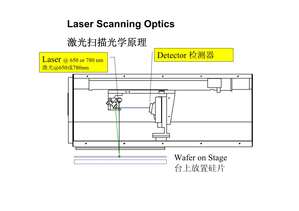
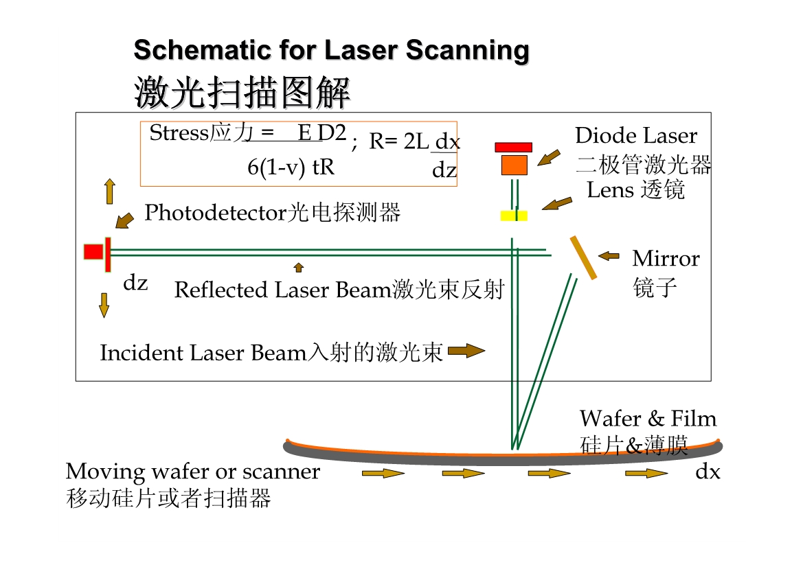
• Dual laser scanner双激光扫描
• Stoney equation for film stress薄膜应力Stoney方程式
• Who needs the products?谁需要这种产品?
• Film property monitor and/or R&D薄膜性能监测及研发
• What are the simple specifications?什么是基本参数?
• Film stress range / reproducibility薄膜应力范围/可再生性
128 Film Stress and Flatness Measurement Models ( Room Temperature )
薄膜应力和平整度测试设备(室温)

Film Stress & Wafer Yield薄膜应力和硅片领域
What causes Film Stress ?什么导致了薄膜应力?
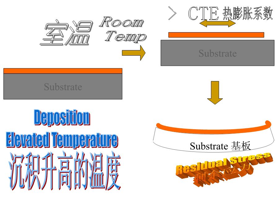
When a thin film is deposited onto a substrate like a flat wafer - mechanical stress will be induced .
薄膜沉积到基板(比如说硅片平面)上时-会产生一个机械应力。
This is exhibited as a wafer bow, where the film will be under tension / “Stress”
这样会表现出一个硅片上的弓起,薄膜就会在张力和压力下。

How Residual Stress is created 剩余应力是如何产生的?
Problems caused by Stress 应力导致的问题
When induced stress exceeds the strength of the deposited film ....
如果产生的应力超过了沉积薄膜的强度….
�Cracking of deposited film沉积薄膜开裂
Delamination & Buckling of film stack薄膜堆栈分层&翘曲
�Metallization hillocks金属化小丘
Voids空隙
All lead to yield loss ($$$)这些导致损失
Principle of Film Stress Measurement 薄膜应力检测原理
Technology for FSM Stress and Wafer bow Measurements
应力和硅片翘曲测量技术
Non Destructive Contactless Method
无损害非接触式方法
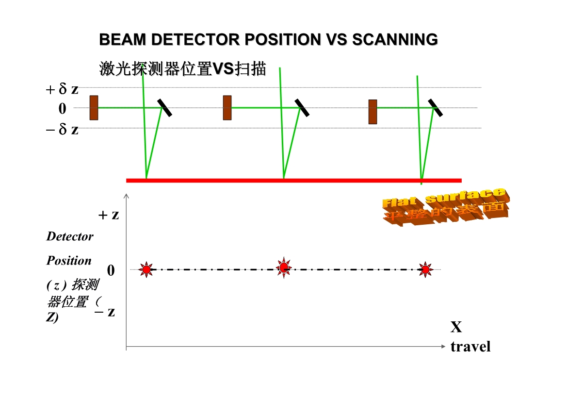
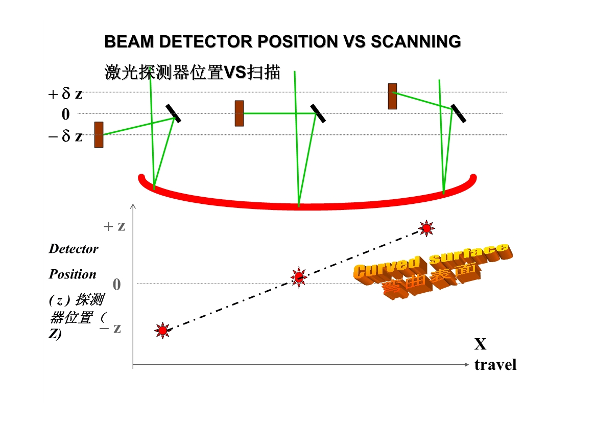
Optilever laser scanning (Patented) Optilever激光扫描(专利)
Procedure for Thin Film Stress Measurement or Map 薄膜应力检测或映射步骤
1. Pre-Measure预检测
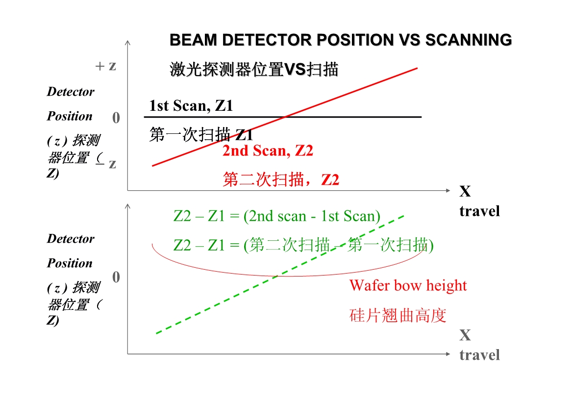
Measure bare wafer surface profile(First Scan or Map )
裸露的硅片表面轮廓测量(第一次扫描或映射)
Deposit Thin Film淀积薄膜
2. Post-Measure后检测
Measure surface profile after film deposition (Second Scan or Map )
薄膜淀积之后表面轮廓测量(第二次扫描或映射)
