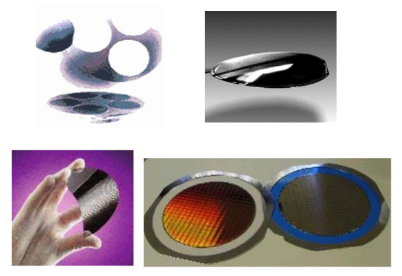
Wafer and Membrane Thickness, Warp, TTV
硅片和薄膜厚度,弯曲,TTV
Optical EchoProbe
光学反射探针
Outline概要
• Introduction简述
• Measurement Requirements for Wafer Thinning硅片减薄测量要求
• Discussion of different approaches for Wafer Thickness Measurement硅片厚度检测不同方法的讨论
• Optical EchoProbe for Wafer Thickness Measurement光学反射探针的硅片厚度检测
• Applications应用
– Thickness and Warp after Grinding, Etching研磨,蚀刻后的厚度和翘曲
– Measurement of stacks of non- and semiconducting materials (MEMS)
–半导体材料(MEMS)的堆叠检测
• Configurations结构
• Summary and Outlook总结和展望
Introduction介绍
History历史
Supplies multiple technologies, for Thickness, global and local Filmstress,Sheet resistance and leakage current, EOT-CV, and adhesion, which are currently being used by the majority of semiconductor fabs and equipment vendors around the globe, including companies like Intel, HP, Freescale, AMD,IBM, TI, Philips, Hitachi, Fujitsu, NEC, Samsung, Hyundai, UMC, TSMC, CSM,Applied Materials, Novellus, among others.
提供多种检测技术,检测厚度,全部和局部薄膜应力,薄膜电阻和渗漏电流,EOT-CV和粘附力,现在大部分的半导体工厂和全球设备供应商都在使用,包括
Intel, HP, Freescale, AMD, IBM, TI, Philips, Hitachi, Fujitsu, NEC, Samsung, Hyundai,UMC, TSMC, CSM, Applied Materials, Novellus,和其它。
Product Portfolio产品系列
●EOT – CV-IV measurements on gate oxide on product wafers硅片栅氧化层CV-IV测量
●RsL – non-contact sheet resistance and leakage current measurements非接触式薄膜电阻和泄漏电流检测
●4pp – 4 point probe for measuring thin metal films薄金属薄膜检测4点探针
●MC – metal contamination measurement金属污染检测
●Raman 360 – strain measurement应变检测
●128 – film stress measurement at room temperature室温下薄膜应力测量
●500 – film stress measurement at 500C 500度下薄膜应力测量
●900 – film stress hysteresis and TDS at 900C (1,100 optional)900度(可选1100度)下磁滞和TDS薄膜应力
●Aquaflex and Laminar – 4 point bend and MELT adhesion testers 4点弯曲和融化粘附性测试
●127 – surface flatness, local, die level and ultra low stress表面平整度,局部,拉模水平和超低应力
●413 and UF800 – wafer thickness, surface roughness, warpage, trench height, bump size measurement (most people use it for insitu thickness monitoring during grinding)硅片厚度,表面粗糙度,翘曲,槽位高度,凸起尺寸测量(很多把它用于研磨时原位厚度监控)
Challenges of Ultra-Thin Wafers
超薄硅片挑战
• Method of Thinning
减薄方法
• Metrologyof Thin wafers
薄硅片度量
• Handling, mounting处理,装配
• Shipping运输
Most Common Measurement Techniques for Wafer Thickness Measurement
硅片厚度检测的一般测量技术
• Capacitance Methods电容方法
• Drop Gauge滴落测量
• Triangulation三角测量
• Low Coherence Interferometry
• 低干扰干涉测量
Capacitance Probes Samples with Tapes 测量胶带硅样电容探针

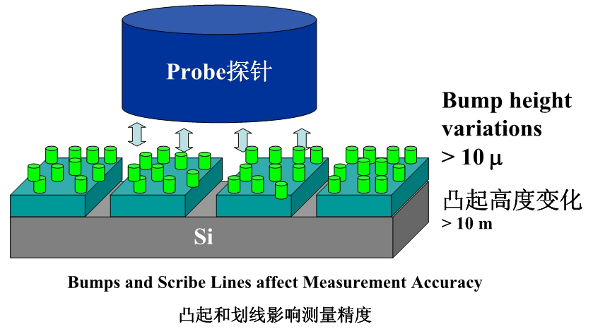
Capacitance Probes affected byBumped Wafers 凸起的硅片影响电容探针

Capacitance Probes电容探针
• Accurate onlyfor bare wafers仅对裸片精确
• Not accurate with patterned wafers对于图案硅片不精确
• Problematic for wafers < 150 microns对硅片的不准确度< 150微米
• Not accurate for wafers with tapes对于带胶带的硅片不精确
• Not accurate with bumped or diced wafers对于凸起的或者切块的硅片不精确
• Does not work with non-conducting materials不适用于不导电材料